Purpose
The RT2825 is a current mode step-down converter with the input voltage range from 4.5V to 18V and provides two channels 5A output current. This document explains the function and use of the RT2825 evaluation board (EVB), and provides information to enable operation, modification of the evaluation board and circuit to suit individual requirements.
Introduction
General Product Information
The RT2825 features two synchronous wide input range high efficiency buck converters that can deliver up to 5A output current from a 4.5V to 18V input supply. The converters are designed to simplify its application while giving the designer the option to optimize their usage according to the target application.
The converters can operate in 5V, 9V, 12V or 15V systems and have integrated power transistors. The RT2825's current mode architecture allows the transient response to be improved. Cycle-by-cycle current limit provides protection against shorted outputs.
Each converter features enable pin that allows a delayed start-up for sequencing purposes, soft-start pin that allows adjustable soft-start time by choosing the soft-start capacitor, and a current limit (RLIMx) pin that enables designer to adjust current limit by selecting an external resistor and optimize the choice of inductor. The COMP pin allows optimizing transient versus dc accuracy response with a simple RC compensation.
The switching frequency of the converters can either be set with an external resistor connected to ROSC pin or can be synchronized to an external clock if needed. The switching regulators are designed to operate from 200kHz to 1MHz. The converters operate with 180° phase between two channels to minimize the input filter requirements.
The RT2825 also features a low power mode enabled by an external signal, which allows for a reduction on the input power supplied to the system when the host processor is in stand-by (low activity) mode.
The RT2825 is available in a VQFN-36L 6x6 package.
Product Feature
- Wide Input Supply Voltage Range : 4.5V to 18V
- Fully Integrated Dual-Buck Converter, Up to 5A/5A
- Adjustable Switching Frequency 200kHz to 1MHz Set by External Resistor or SYNC Signal
- Dedicated Enable/Soft-Start for Each Buck
- Current Mode Control with Simple Compensation Circuit
- Adjustable Cycle-by-Cycle Current Limit Set by External Resistor
- Over-Temperature Protection
- Power Good Indicator
- Discontinuous Operating Mode at Light Load when LOWP pin = L
- 1% VREF Accuracy
Key Performance Summary Table
|
Key Features
|
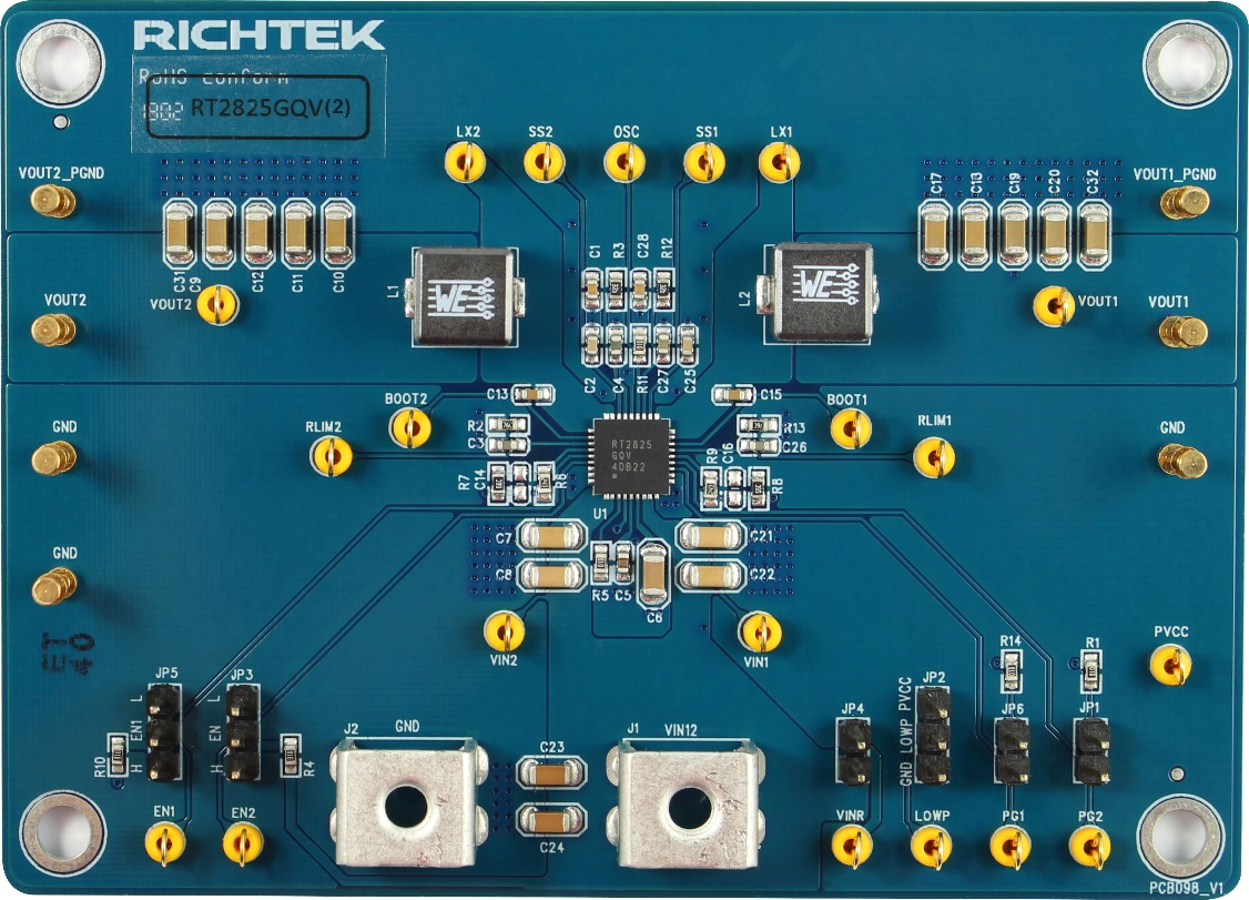
Evaluation Board Number : PCB098_V1
|
|
Default Input Voltage
|
12V
|
|
Max Output Current
|
IOUT1 = 5A; IOUT2 = 5A
|
|
Default Output Voltage
|
VOUT1 = 1.8V; VOUT2 = 1.8V
|
|
Default Marking & Package Type
|
RT2825GQV(2), VQFN-36L 6x6
|
|
Operation Frequency
|
Adjustable Frequency. Default = 400kHz
|
Bench Test Setup Conditions
Headers Description and Placement
Carefully inspect all the components used in the EVB according to the following Bill of Materials table, and then make sure all the components are undamaged and correctly installed. If there is any missing or damaged component, which may occur during transportation, please contact our distributors or e-mail us at evb_service@richtek.com.
Test Points
The EVB is provided with the test points and pin names listed in the table below.
|
Test point
|
Signal
|
Comment (expected waveforms or voltage levels on test points)
|
|
VIN1, VIN2
|
Power Input Voltage Test Point
|
To monitor the voltage of input capacitors.
|
|
VINR
|
Signal Power Input Test Point
|
To monitor the voltage of internal control circuit.
|
|
EN1, EN2
|
Enable Test Point
|
To monitor enable control input voltage of CH1 and CH2. A low level signal on this pin disables it. If this pin is left floating, a weak internal pull-up will allow automatic enables.
|
|
LOWP
|
Low Power Mode Test Point
|
To monitor the control voltage of LOWP pin.
|
|
PG1, PG2
|
Power Good Test Point
|
To monitor power good signal of CH1 and CH2.
|
|
RLIM1, RLIM2
|
Current Limit Test Point.
|
To monitor the voltage of RLIM1/RLIM2 pins.
|
|
BOOT1, BOOT2
|
Bootstrap Supply Test Point
|
To monitor the voltage of BOOT1/BOOT2 pins.
|
|
LX1, LX2
|
Switch Node Test Point
|
To monitor the switching voltage of CH1 and CH2.
|
|
SS1, SS2
|
Soft-Start Test Point
|
To monitor the SS voltage of CH1 and CH2.
|
|
OSC
|
Oscillator Setting Test Point
|
To monitor the voltage of OSC pin.
|
|
VOUT1, VOUT2
|
Output Voltage Test Point.
|
To monitor the output voltage of CH1 and CH2.
|
|
GND
|
Ground
|
Ground.
|
|
PVCC
|
Internal Regulator Output Test Point.
|
To monitor the 5V power supply output voltage of PVCC pin.
|
Power-up & Measurement Procedure
1. Connect input power (4.5V < VIN < 18V) and input ground to VIN12 and GND respectively.
2. Connect positive end and negative terminals of load to VOUT1/VOUT2 and VOUT1_PGND/VOUT2_PGND respectively.
3. There is a 3-pin header “EN” for enable control. To use a jumper at “H” option to tie EN test pin to input power VIN via a 100k resistor for enabling the device. Inversely, to use a jumper at “L” option to tie EN test pin and ground GND for disabling the device. Let EN floating will also enable control.
4. Verify the output voltage (approximately 1.8V) between VOUT1/VOUT2 and GND.
5. Connect an external load up to 5A to the VOUT1/VOUT2 and GND terminals and verify the output voltage and current.
Output Voltage Setting
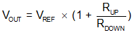
Set the output voltage with the resistive divider (RUP = R7, R8; RDOWN = R6, R9) between VOUT and GND with the midpoint connected to FB. The output is set by the following formula :
Frequency Setting
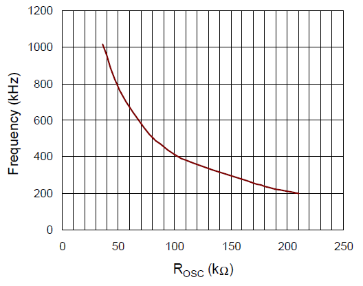
Set the converter frequency with the oscilator resistor (ROSC = R11) between OSC and GND. The practical switching frequency ranges from 200kHz to 1MHz. Determine the ROSC resistor value by examining the curve in below Figure.
Schematic, Bill of Materials & Board Layout
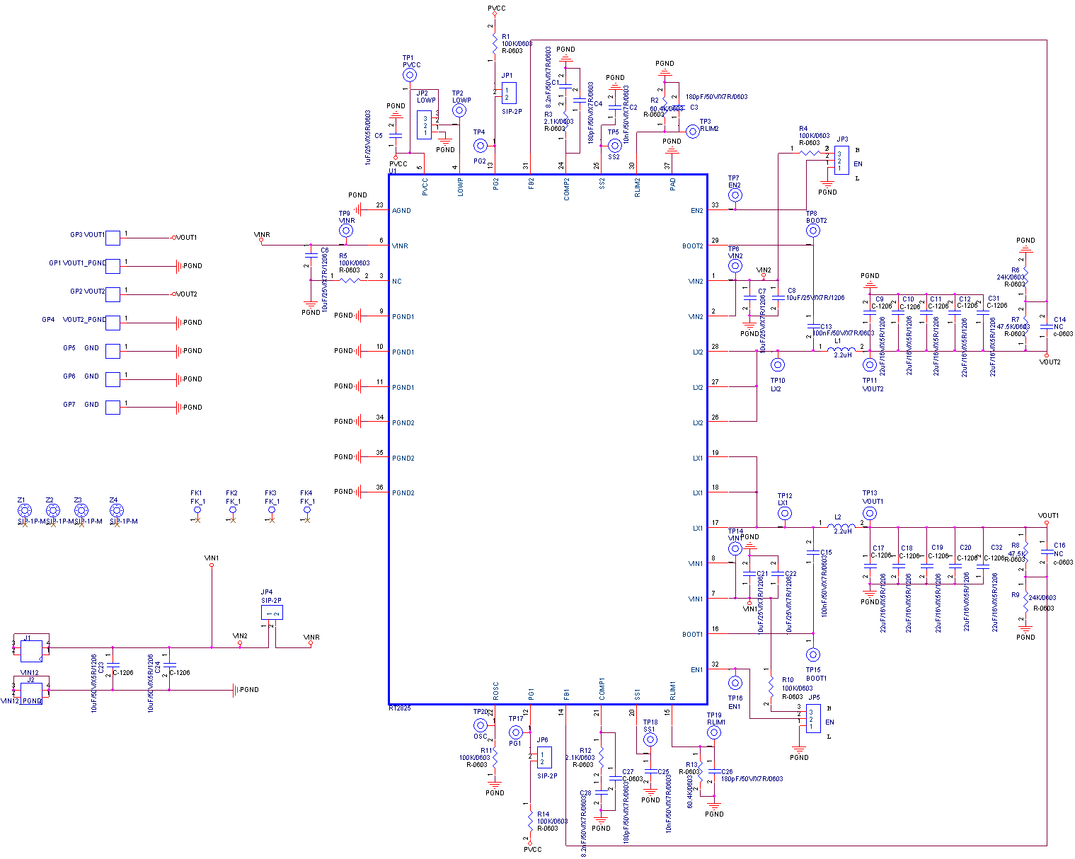
EVB Schematic Diagram
Bill of Materials
|
Reference
|
Qty
|
Part Number
|
Description
|
Package
|
Manufacturer
|
|
U1
|
1
|
RT2825GQV(2)
|
DC-DC Converter
|
VQFN-36L 6x6
|
RICHTEK
|
|
C1, C28
|
2
|
0603B822K500CT
|
8.2nF/50V/X7R
|
C-0603
|
WALSIN
|
|
C2, C25
|
2
|
C1608X7R1H103KT000N
|
10nF/50V/X7R
|
C-0603
|
TDK
|
|
C3, C4, C26, C27
|
4
|
0603B181K500CT
|
180pF/50V/X7R
|
C-0603
|
WALSIN
|
|
C5
|
1
|
TMK107BJ105KA-T
|
1µF/25V/X5R
|
C-0603
|
TAIYO YUDEN
|
|
C6, C7, C8, C21, C22
|
5
|
GRM31CR71E106KA12L
|
10µF/25V/X7R
|
C-1206
|
muRata
|
|
C9, C10, C11, C12, C17, C18, C19, C20, C31, C32
|
10
|
GRM31CR61C226KE15L
|
22µF/16V/X5R
|
C-1206
|
muRata
|
|
C13, C15
|
2
|
GRM188R71H104KA93D
|
100nF/50V/X7R
|
C-0603
|
muRata
|
|
C23, C24
|
2
|
C3216X5R1H106K160AB
|
10µF/50V/X5R
|
C-1206
|
TDK
|
|
L1, L2
|
2
|
7443330220
|
2.2µH
|
L-8-4x7-9
|
WURTH ELEKTRONIK
|
|
R1, R4, R5, R10, R11, R14
|
6
|
WR06X1003FTL
|
100k
|
R-0603
|
WALSIN
|
|
R2, R13
|
2
|
WR06X6042FTL
|
60.4k
|
R-0603
|
WALSIN
|
|
R3, R12
|
2
|
RTT032101FTP
|
2.1k
|
R-0603
|
RALEC
|
|
R6, R9
|
2
|
WR06X2402FTL
|
24k
|
R-0603
|
WALSIN
|
|
R7, R8
|
2
|
RTT034752FTP
|
47.5k
|
R-0603
|
RALEC
|
Measurement Results
PCB Layout
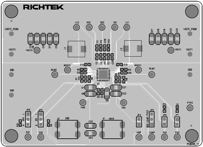
Top View (1st layer)

PCB Layout—Inner Side (2nd Layer)

PCB Layout—Inner Side (3rd Layer)
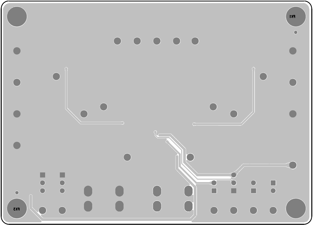
Bottom View (4th Layer)